Previous article
Common Parts Library now on Github!
Octopart Staff
Recently, we’ve written about the current state of desktop electronics manufacturing and one click manufacturing. Continuing this discussion, we want to explain how the Common Parts Library (CPL) can be used to find parts for a printed circuit board design. The CPL is a list of commonly used parts for prototyping, designing, and manufacturing connected device products. This comprehensive list makes it easy and fast to choose the parts you are looking for—passives, interface ICs, connectors, and more—and provides information like stock availability, pricing, and symbols and footprints. In this blog, I will talk about how I used the CPL for designing a PCB of my own.
As a graduate student at Columbia University, I got the chance to design an IC from scratch. The idea was to make an integrator-based voltage regulator—to convert voltage into frequency information using oscillators and then convert it back to voltage—which seemed like an interesting problem, and it was a fantastic chance to test out the idea on an actual IC. A potential application of this IC can be in low-power biomedical applications like pacemakers.
We used 180nm technology using the MOSIS fabrication process. MOSIS is a student-friendly service, and they keep costs low by aggregating multiple designs onto one mask set.
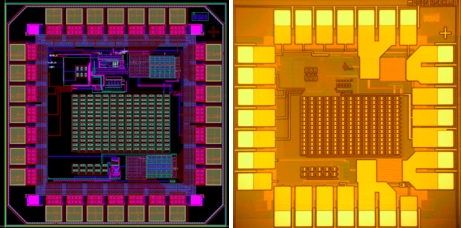 Left: Silicon mask in design software - Cadence Virtuoso, Right: Photograph of the actual IC
When the IC came back after the summer, it looked like this:
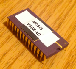 A custom designed IC
Next, a PCB had to be made to test the chip to see whether it was regulating the output voltage. For the PCB, we had to design a current biasing circuit and also design the load of the regulator. These were the requirements:
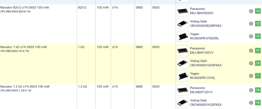
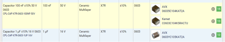
Below is the summary of our part selection:
For surface mount resistors, we used Panasonic's ERJ-3EKF series.
For decoupling capacitors, we used Kemet’s C0603C series.
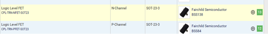
For transistor, we wanted a fast switching NMOS and went for Fairchild Semiconductor’s BSS138.
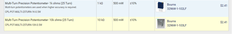
For the through-hole multi-turn potentiometers, we went for Bourns’ 3296W series.
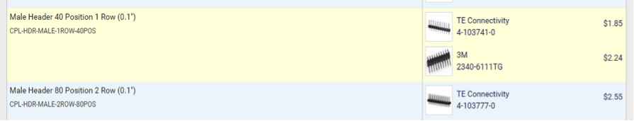
For the headers and test points, we found 3M’s headers and Keystone’s test points.
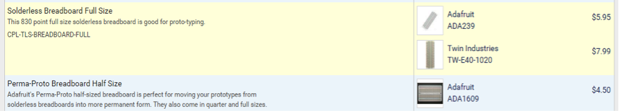
For breadboards, we used Twin Industries’ breadboard.
Our first board looked like the one below. We were very conservative and left plenty of space in case something went wrong. Indeed, we found out that we hadn’t placed a potentiometer to adjust the load current, and we had to solder it back in later.
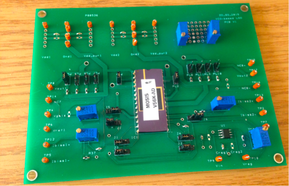 The first prototype PCB for testing our IC
We tested the IC and, for the most part, it worked well. The next step was to make a more usable and compact PCB. We used Altium Designer for the new PCB design. Like the first prototype, we used the CPL to get the parts for the board. We moved all the test points to the edges of the board, made all switches symmetric and left some space for headers in case we had to solder something back in later. Our final PCB looked like this:
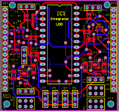 The PCB design of our second prototype using Altium Designer
Here is the photo of the unassembled PCB of this prototype:
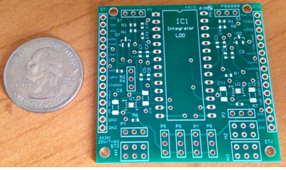 The second prototype PCB for testing our IC